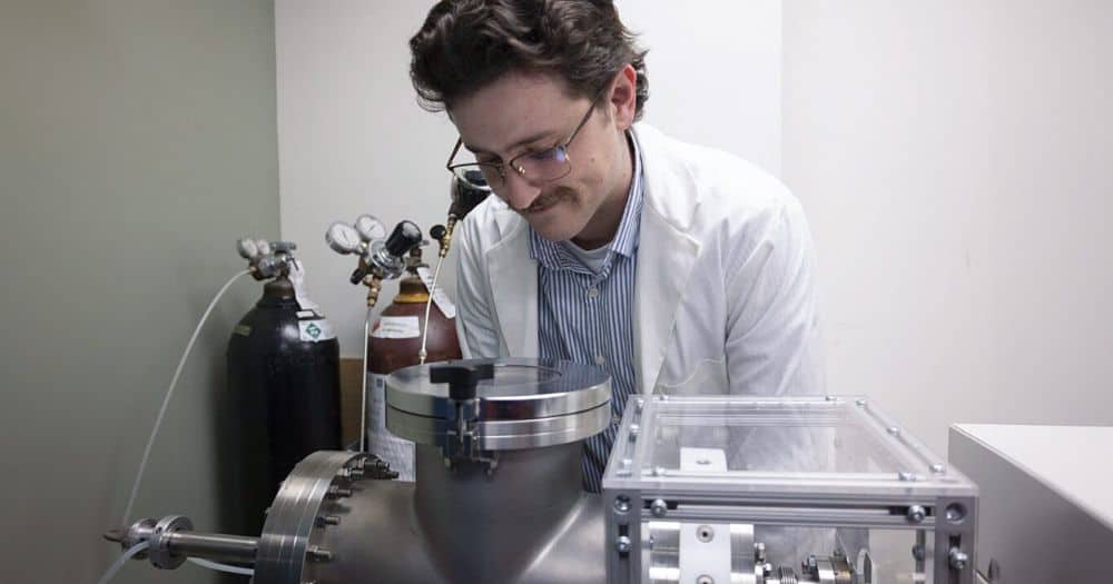
[Image above] Noah Stocek, Ph.D. student at the University of Western Ontario, looks inside the customized remote plasma deposition system he designed with physics professor Giovanni Fanchini and assembled with postdoctoral fellow Farman Ullah. Using this system, they produced new record-setting 2D auxetic materials. Credit: Mitch Zimmer, University of Western Ontario
By Laurel Sheppard and Lisa McDonald
When too many projects pile up at work, people often use the metaphor “stretched thin” to describe their struggle to dedicate adequate attention to each task. This expression is based off the well-known behavior of elastic materials, which will expand out in the direction of an applied force (each of the new projects) at the cost of becoming very thin in the crosswise direction (fewer hours for each task).
What if, by some miracle, the addition of more projects could increase the number of hours available for each task? Though this suggestion is just wishful thinking for overwhelmed workers, a special class of materials known as auxetic materials do exhibit this counterintuitive behavior by becoming thicker in the direction perpendicular to an applied force.

In addition to their unusual strain behavior, auxetic materials demonstrate excellent vibration absorption and stronger indentation resistance than elastic materials. These properties make auxetic materials attractive for use in impact engineering applications.
Auxetic materials are commercially available as polymeric foams and fabrics, and researchers anticipate these materials will soon find wider application in areas such as textiles and electromechanical systems. Realizing these potential applications, though, will require the development of other materials that exhibit auxetic behavior, such as metallic foams, carbon fiber laminates, and novel graphene nanostructures.
Two-dimensional metallic auxetics are especially interesting because they are expected to offer both flexibility and high lateral charge mobility, as well as have the capability to compensate for thermal expansion at the nanoscale. These properties would be useful in wearable electronics.
Of the 2D metallic auxetics, 2D tungsten semicarbide (W2C) was theoretically predicted to exhibit extreme auxetic behavior. However, it is difficult to synthesize this material because most carbide growth techniques operate close to thermodynamic equilibrium, resulting in the formation of conventional tungsten carbide (WC) instead.
In a paper published in April 2024, researchers at the University of Western Ontario, led by physics professor Giovanni Fanchini, came up with a solution to synthesize W2C. Instead of the typical chemical vapor deposition approaches, they designed a dual-zone, ultrahigh-vacuum, remote plasma deposition system.
Conventional plasma deposition techniques for thin films and 2D materials involve placing the substrate directly within a plasma chamber and using a gas discharge to provide the energy for material growth reactions.
In contrast, remote plasma-assisted techniques extract the plasma from the plasma chamber, and species that travel far enough to reach the substrate are deposited. The remote plasma process allows the growth of tungsten carbides outside of equilibrium thermodynamic conditions.

Using this system, the researchers successfully produced 2D flakes of W2C. Their achievement depended on identifying the specific deposition conditions for which hydrocarbon precursors (W2CHn) can be remotely extracted from the plasma.
First, using optical emission spectra, they investigated how the amount of argon backflow affected the reactor behavior. They determined that if there was no backflow, the amount of exposed tungsten on the surface that can be sputtered was reduced, leading to a large area of WC. For a slightly higher backflow, the rate of decomposition from CH4 to CH+ increased proportionally, but a substantial portion of the target’s surface still showed WC formation.
At a backflow rate of 3 standard cubic centimeters per minute (sccm), a more uniform texture was observed, which resembled the crystallographic structure of single-layer W2C. Increasing the backflow to 5 sccm led to a higher deposition rate and flake thickness, but beyond that, the diffusion of W2CHn species started to be limited again, thus reducing the deposition rate.
Investigation of the 2D W2C flakes revealed that these materials exhibited the strongest experimentally observed auxetic behavior observed to date, expanding by up to 40% under applied strain. This expansion is four times more than the previous experimental record observed in 2D black phosphorous.
In addition, the researchers developed a transfer printing method to move the W2C flakes without damage. This method involves first spinning a polymer acetone solution onto a copper substrate. After several other steps, the coating can be removed from the substrate and stamped onto a new substrate, followed by a heating step that adheres it to the substrate. Another heating step removes the polymer, leaving assemblies of W2C flakes on the substrate. The authors believe this method is effective in transferring isolated, well-defined flakes, which can then be used in mechanically switchable photonics crystals and oscillators.
The researchers conclude, “Our experimental demonstration of giant auxetic behavior of [few-layer W2C] represents a unique contribution toward the application for 2D materials.”
The paper, published in Materials Horizons, is “Giant auxetic behavior in remote-plasma synthesized few-layer tungsten semicarbide” (DOI: 10.1039/D3MH02193A).
